Transistors are devices that are used to drive output transducers. They deal with electrical power in response to electrical signals.
The above is a fairly concise description of what transistors do. By considering a systems approach to electronics, processes such as counters and logic circuits often need to drive larger output devices such as bulbs, motors and heaters etc. The devices used to perform the various processes are often small low power ICs that can only source or sink relatively small currents (several mA) and work at fairly low voltages. The output transducers may, on the other hand, require larger currents (several Amps) and work at higher voltages. Something needs to allow the process devices to work with the output transducers and this is where transistors are used.
Transistors are devices that require only small input currents or voltages but can handle large output currents.
There are two distinct types of transistor, the bipolar transistor and the MOSFET, and for each type of transistor there are two varieties. Bipolar transistors can be either npn type or pnp type. Bipolar transistors are devices that are operated by current. MOSFETs are operated by voltages and can be either n-channel or p-channel MOSFETs. As transducer drivers, MOSFETs tend to be better at handling high currents than bipolar transistors but bipolar transistors are better suited to low voltage circuits.
 An npn bipolar transistor is an active circuit component with three legs and usually made from silicon. The simple npn bipolar transistor can be used to construct all of the logic gates, and by extension all digital circuits, and also Op-Amps and all manner of analogue circuits. The npn bipolar transistor is therefore a fundamental building block of modern electronics.
The npn bipolar transistor can also be used as a straightforward electronic switch. Used as a switch, or transducer driver, the transistor can be used to control powerful devices and switch large currents. A basic electronics course only considers this simple application as a transducer driver.
 An npn bipolar transistor has three terminals or, in other words, three legs.
These are called the Base,Collector and Emitter. The emitter is identified by the arrow pointing outwards.
Basic action: When a small current flows into the Base, a much larger current is allowed to flow from the Collector to the Emitter. To enable a Base current to flow, the Base potential must be 0.7 V higher than the Emitter potential.
The bipolar transistor is a current operated device.
Bipolar transistors come in different shapes and sizes depending on their intended use.
 Signal transistors are used for signal processing, logic operations and voltage amplifiers. They come in a small metal canister style package (e.g. BC108) or a small plastic package (e.g. BC456). On the canister type, the tag on the case marks the emitter and the metal case is connected to the collector.
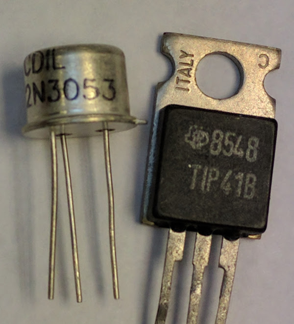 Medium sized transistors also come as a slightly larger metal can type or as a TO-220 style plastic type with a metal mounting tag. Examples include 2N3053, BC441 and TIP41B. Again, the emitter is marked by a tag on the metal case and the metal case and metal heatsink tab are connected to the collector. These are used as transducer drivers and low power amplifiers and are capable of handling currents of 1 or 2 amps.
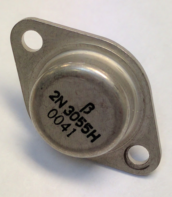 Power transistors can handle large currents and are used in high power amplifiers and high current regulators. Examples of power transistors include the well known 2N3055.
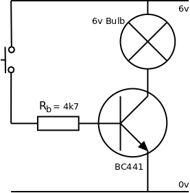 The circuit shows an npn bipolar transistor connected as a transducer driver.
When the button is pressed the Base voltage is greater than 0.7 V and so current flows through the Base resistor and into the Base. The resistor is necessary to allow the Base-Emitter voltage to remain at 0.7 V. As a small current is flowing into the Base, a larger current is allowed to flow from the power rail, through the bulb, into the Collector and out through the Emitter to 0 V. The bulb is ON.
With the button not pressed, no current flows into the Base and no current flows through the Collector to the Emitter. The bulb is OFF. When there is no Base current, the resistance between the Collector and Emitter is very high. When current flows into the Base, the Collector-Emitter resistance drops and allows current to flow.
 When an npn bipolar transistor is used to control a motor, solenoid, relay or any other device containing an electromagnet, a protection diode is necessary to protect the transistor from the large back e.m.f. produced when the device is switched off.
Note: In all cases a low power circuit (such as a logic gate) controls the transistor and the transistor controls the high power device (such as the bulb or motor).
 To turn the transistor on, the potential difference between the Base and Emitter must be 0.7 V. Therefore, it makes sense to always connect the Emitter directly to 0 V so that any Base voltage above 0.7 V applied to the Base resistor will turn the transistor on. This is how the npn bipolar transistor is always connected when used as a transducer driver.
 The npn bipolar transistor can be thought of as a current amplifier. A small Base current is amplified to give a large Collector current. The Current Gain (hFE) is given by the ratio of the Collector current to the Base current.
The current gain of a typical signal transistor is between 100 and 200 and is less for a power transistor. Current gain can be measured directly with a suitable multimeter.
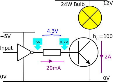 The Base resistor is important. Consider the example in the diagram.
Step 1. The power rating of the bulb tells us the required Collector current is 2 A.
Step 2. The transistor current gain is x100 therefore the necessary Base current is 2 ÷ 100 = 20 mA
Step 3. The input voltage is 5 V and the Base-Emitter voltage is 0.7 V, therefore, the potential difference across the Base resistor is 5.0 − 0.7 = 4.3 V
Step 4. The resistor equation gives RBase = 4.3 ÷ 0.02 = 215 Ω
Step 5. To ensure the transistor is fully turned on, use the next lowest E24 series resistor.
Step 6. Choose RBase = 210 Ω
To understand how the npn bipolar transistor behaves, a simple circuit can be used. The input voltage is varied which varies the Base current. The Collector current and the voltage across the transistor (potential difference across the Collector and Emitter) can be measured. The relationships between the input voltage or current and the output voltage or current are known as the transfer characteristics and describe how the transistor functions.

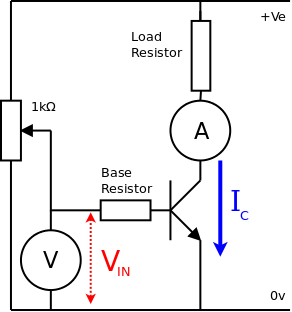
 The circuit shown can be used to investigate the transfer characteristics of an npn bipolar transistor. The potentiometer allows the input voltage to be varied. VIN and VCE (the voltage between the Collector and the Emitter) are measured using voltmeters.
The transfer characteristics of a device describe how the output changes as the input changes. In this case the transfer characteristics of the bipolar transistor describe how the Collector-Emitter Voltage VCE depends on the input Voltage VIN to the Base resistor.
When the input voltage is less than the transistor turn on voltage of 0.7 volts (region 1) no current flows through the base resistor and no current flows through the transistor from the Collector to the Emitter. The potential difference across the load is zero (V = I x R and I = 0 therefore V = 0) and the Collector-Emitter voltage equals the supply voltage.
When the input voltage is just above 0.7 volts there is a potential difference across the Base resistor and a small current flows into the Base of the transistor. As a result, current flows through the load resistor and into the Collector. The current is limited by the transistor because the small Base current only allows a limited Collector current. VCE = Vsupply − Vload. The Collector-Emitter voltage is not close to zero and the Collector current is not zero so the bipolar transistor dissipates power and may get hot or be damaged (region 2).
When the input voltage is well above 0.7 volts (region 3) a larger current flows through the Base resistor and now the Collector current is limited by the load resistor. All of the supply voltage is dropped across the load resistor and the Collector-Emitter voltage is (almost) zero. When the transistor is used as a transducer driver, VIN must be high enough (depending on load current and current gain of the transistor) such that VCE is close to zero.
Note: This circuit, using two resistors and a transistor, is a NOT gate. When VIN is LOW, VOUT is HIGH and vice versa.
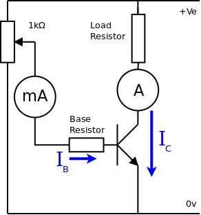
 The circuit shown can be used to investigate the transfer characteristics of an npn bipolar transistor. A voltmeter measures VIN and an ammeter in series with a load resistor measures IC. The load resistor limits the maximum Collector current and means the transistor is acting as a transducer driver with the load resistor acting as the transducer.
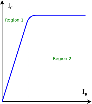
In this second case the transfer characteristics of the bipolar transistor describe how the Collector Current IC depends on the Input voltage VIN.
In region 1, VIN is less than the 0.7 volts, the transistor does not conduct and IC is zero.
In region 2, VIN > 0.7 volts, current flows into the Base and the transistor conducts. The Collector current depends on the current gain of the transistor and this part of the transfer characteristic is linear. The greater the current gain, the steeper the line.
Region 3 is when VIN is large enough so that enough current flows into the Base of the transistor to allow enough current to flow through the transistor and the load resistor to make the potential difference across the load resistor the same as the supply voltage. VCE is zero and the Collector current cannot be any greater because it is limited by the load resistor.
 The circuit can be used to investigate the current gain of an npn bipolar transistor. The small Base current is measured with a milliammeter and the larger Collector current measured with an ammeter.
In region 1, increasing the Base current IB allows a larger current to flow through the Collector IC and the graph is linear and passes through the origin. This section of the graph can be described by the equation of a straight line where the gradient is known as the current gain (hFE) of the transistor. The Collector current is directly proportional to the Base current. In region 1 the equation relating IC and IB is:
In Region 2, the current is limited by the load resistor. The maximum current is given by Vsupply ÷ Rload and changing the Base current has no effect on the Collector current.
Configured as a transducer driver, this is the most basic application of an npn bipolar transistor. Although it is acceptable to think of the transistor as a simple electronic switch in this case, there are many more complex applications where this simplistic approach is not appropriate.
© Paul Nicholls
March 2018

Electronics Resources by Paul Nicholls is licensed under a Creative Commons Attribution 4.0 International License.